I've been thinking about redesigning my Williams multigame for years, but I just hadn't gotten around to it. I discussed various possibilities with different people, and came up with the idea of a single board that would plug in between the CPU and ROM boards. Nearly every necessary signal is available on that connector, so very little modification would have to be done to the boards.
For a while I considered just replicating all my hacks on a single board, but decided that wouldn't be very interesting. I knew about PALs, PLDs and FPGAs, but never really considered learning how to use them. Then I read an article in the January 2004 issue of Nuts & Volts magazine about the Intro-FPGA from HVW Technologies.
I bought a couple of the kits and played with them, and quickly decided that was the way to go. Altera provides free design software; I chose to use schematic capture, where you draw the circuits in their program and it creates the programming for the chip. Then you connect a cable from your printer port to the circuit and upload the design. If you made a mistake or want to make a change, you edit the schematic and upload the new design.
I also wanted to simplify my control panel switcher. There are 17 button and joystick inputs from my multigame control panel that need to be switched to 19 different inputs on the "widget" PIA board. I had been using a bunch of 4066 analog switches, but it was messy and completely inflexible. If I ever wanted to change anything, I had to rewire that board. I had considered using a PIC microcontroller, but I wanted to introduce no latency, so I decided to use another FPGA. But the Altera 7064SLC-44 that comes with the Intro-FPGA only has 32 I/O pins available, so I needed a larger device. I wound up buying some 7064SLC-84's. This is the identical device, but in a larger package, so there are more I/O pins. The same Altera software and programming cable work with it.
The control panel switcher design is pretty simple- logically AND together the game select signals with the corresponding inputs, and logically OR the matching outputs together. My original circuit connected to the existing widget board in the game, but that board has to be modified to play Sinistar, since that game uses an input that no other game uses. I started thinking about how to get it working without modifying that board, and finally hit on the idea of removing the widget board altogether. Its function is to multiplex inputs to the CPU board, which is what my control panel switcher does. Moving the widget functionality to my new board meant that the existing widget board didn't have to be modified- in fact, it is removed completely, and my new board in bolted in its place.
The widget board has a 6821 PIA chip and two 74257 multiplexers as well as some inverters and a bunch of resistors and capacitors. Luckily, the PIA is only used for input, so I didn't have to create all the configurable I/O or interrupt circuitry.
Another alternative would be to create a programmable crosspoint switch with an FPGA and have the menu software configure it before starting the game. That would make changing things even easier.
Currently, I'm running 13 different games: Joust, Defender, Stargate, Splat, Robotron, Bubbles, Sinistar, Lotto Fun, Mayday, Colony 7, PlayBall, Speed Ball, Alien Arena. The ROM has room for 16 images, but one is used for the menu, so I've got 2 more spots open. Right now, I've got the pterodactyl-cheat Joust in one and Defender II (Stargate from Williams Arcade Classics) in the other. Colony 7 and PlayBall are vertically-oriented games, so they are rotated clockwise like Sinistar, but all 3 are playable.
The Defender-like games (Defender, Colony 7, Mayday) are still a bit of a problem- 2 addresses on the CPU board are different from the other games (VIDCTRS is at $CB00 on Joust and $C800 on Defender, while the watchdog is at $CBFF on Joust and $C3FC on Defender). Since they are on the CPU board, my hack can't intercept them, so the only options are to hack the CPU board or patch the ROMs. You could disable the watchdog, but I didn't want to; I decided to recreate the watchdog circuit in one of the FPGAs. That way I could use the correct address/data trigger for each game. I also implemented a game reset by holding the watchdog output low when the left joystick is pressed up and both player 1 and 2 start buttons are pressed.
There's still a problem, though- the Joust boardset only decodes the high 6 bits of the address to create the _$C000 signal that triggers writing the color registers. That means that writes to $C3FC, the Defender watchdog address, get stored as color 12. This is the cause of the screen glitches that I get when I start Defender. I'm still confused why they go away; my current guess is that while the game is playing, the watchdog is cleared only during the vertical blanking period, so the glitch happens off the screen. But color 12 is constantly being loaded with $38, bright green.
Normally the 74154 on the ROM board decodes the high 4 address bits and provides active-low signals for each 4K page. 12 of those are used to select ROMs, and 1 is the _IO signal. Since Defender bank switches ROM and I/O into the $Cxxx space, I can't use the Joust ROM board's signal, so I have to create the _IO signal myself and send it to the CPU board.
I fixed the Defender watchdog/color 12 problem by splitting the _IO signal from my circuit into _IO_CPU and _IO_FPGA. _IO_FPGA is the same as the old _IO signal- it's low whenever I/O locations are accessed. This is any time $Cxxx is accessed in the later games, and when $Cxxx is accessed in page 0 while running Defender. It's used by the other FPGA to handle I/O. _IO_CPU is the signal that gets routed to the CPU board. I make it high whenever the $C3xx range is accessed, eliminating the graphics glitches.
I used the same idea to disable the onboard CMOS highscore RAM. A circuit makes _IO_CPU high whenever the range $CC00-CFFF is accessed, so the IC is never selected, and the CPU board doesn't need to be modified.
There is still one problem, though. When Defender addresses ROM in the $Cxxx area, the Joust ROM board generates the _IO signal. This is no longer fed back to the CPU board, but if the range is $C800-$CBFF, the ROM board selects the PIA, the screen flip hardware, or the special chips. So when Defender tries to read $C800, the PIA asserts its signals, which fight with the multigame's ROM. Originally I got around this by cutting the trace from the 74154 and feeding my _IO signal from the FPGA to the ROM board. In order to fix this issue without modifying the ROM board, I used the A10/A3/A2 inversion hardware in the FPGA. That circuit normally converts access to the Defender ROM PIA at $CC00-3 to the Joust ROM PIA at $C80C-F by inverting 3 address bits. Now it also inverts those bits when Defender addresses the range $C800-$CBFF, converting those addresses out of the area where the Joust ROM board decodes.
VIDCTRS (short for video counters) is an address that returns the high 6 bits of the counters that drive the video generation. This way, the CPU can know approximately where on the screen the CRT is drawing. This is especially nice to avoid flicker by doing updates during the vertical blank interval. On the Joust CPU board, VIDCTRS is at $CB00 (actually $CBxx where xx is even), but on the Defender CPU board, address $C800 is used. Since the address decoding takes place on the CPU board, my multigame can't intercept it like the ROM board signals. I originally addressed this issue by creating a signal on one of the FPGAs that I routed back to the CPU board. It was low when $C800 was read during Defender, and low when $CB00 was read during the other games. But that required cutting a trace. Since the #1 goal of the new multigame is to not modify any hardware, a patch is needed.
My original multigame (revision 0) ran a highly patched Defender, and VIDCTRS was one of the items I patched for. But another goal of the new multigame is to patch as little code as possible. One reason is that I want to be able to run multiple versions of games without having to spend a lot of time disassembling code to figure out where to apply patches. Also, copy protection code could cause a problem if it finds a patch, so the fewer and the smaller the patches, the better. There are 3 accesses to VIDCTRS in Defender, all in the same 4K chunk. I needed to make sure the patch kept the ROM checksum the same, so that the game wouldn't display a ROM error during initial tests. This checksum routine is pretty simple- it just adds each byte together (with carry), discarding overflow. To fool it, you need to change another byte so that the differences cancel out. I took advantage of the fact that the games (and the multigame) don't fully decode every I/O address. If you look at the Joust CPU schematics, VIDCTRS is accessed using address bits 15 through 8 and 0. It doesn't matter what address bits 7 through 1 are. The games use $CB00, but any even number from $CB00 to $CBFE will work. I patched the first 2 instances of $C800 to $CB00. This added 6 to the checksum. I patched the next instance of $C800 to $CBF6. $C8 to $CB added 3 more, but $00 to $F6 subtracted 10 and added 1 (because of the carry). The net sum is zero, so the checksum routine is fooled. (Note that the more sophisticated checksum routines in MAME do notice the difference.) This VIDCTRS patch requires no hardware hack, and only affects 12 bits in 4 bytes, meeting my goals.
I had to patch Mayday's protection scheme to get it to work. There are a few details in the MAME source code. It turns out there are a couple of comparisons you need to patch. Again, I worked out a "checksum-preserving" patch using the "branch never" opcode. I also had to use the Defender sound ROM instead of Mayday's; there are only 2 bytes that are different, and the Mayday file didn't work.
Neither Colony 7 nor Alien Arena allow free game play, so I created a signal that is grounded when the left joystick is pressed up and the player 1 start button is pressed. I wired this to the ROM PIA input for the left coin slot, so I can add credits to any game. I also intercepted the _HALT line from the ROM board to the CPU board, and I can latch it by pressing the left joystick up and the player 2 start button. This gives me a pause button that works in all the games. Everything is frozen unless I press the player 2 start button, which temporarily allows the CPU to run. This lets me "slow-mo" by tapping the button. To restart, first I hit player 1 start, then move either joystick left or press any of the 4 buttons closest to the 2 joysticks. The idea is to make the player hit a non-gameplay button (player 1 start) so they won't accidentally take the game off pause, then wait for them to get their hands back into position before restarting. If you just had to hit player 1 start to restart, you then have to move your hands quickly back into position, which could cause you to lose a life. This way, you get your hands into position then move a joystick or press a button to restart. It seems to work very well.
PlayBall has a Sinistar-like sound board with CVSD for voice. The ROMs are organized a little differently, though. I had to double the size of my speech EPROM and create a new signal to select which half to use.
Speed Ball requires trackballs; I'm trying to emulate them in the FPGA with the joysticksm but I'm running out of resources. I guess I'll look at a bigger FPGA.
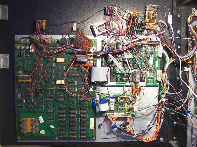
Here's a pic of my old hacks. Every hack was on a different board, and there were wires everywhere.
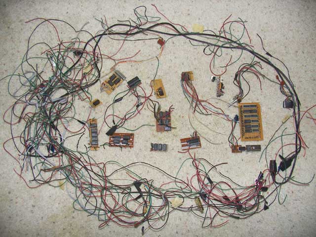
Here are all the hacks and wires cut off.
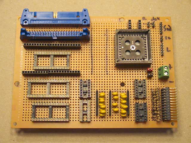
Here is the front of my new hack board.
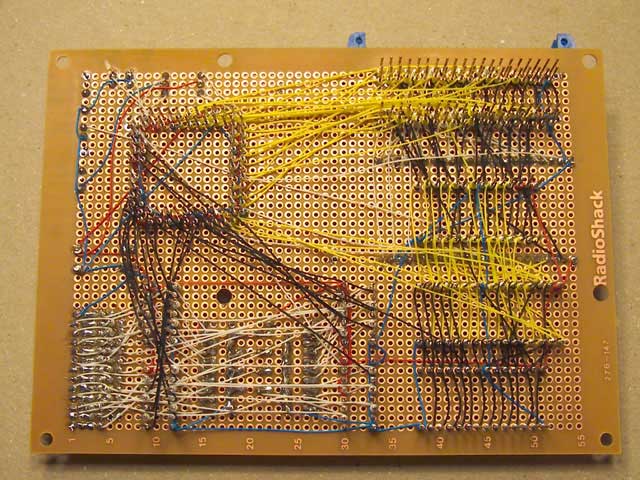
Here is the back of my new hack board.
Here is the schematic of the smaller FPGA.
Here is the schematic of the larger FPGA.